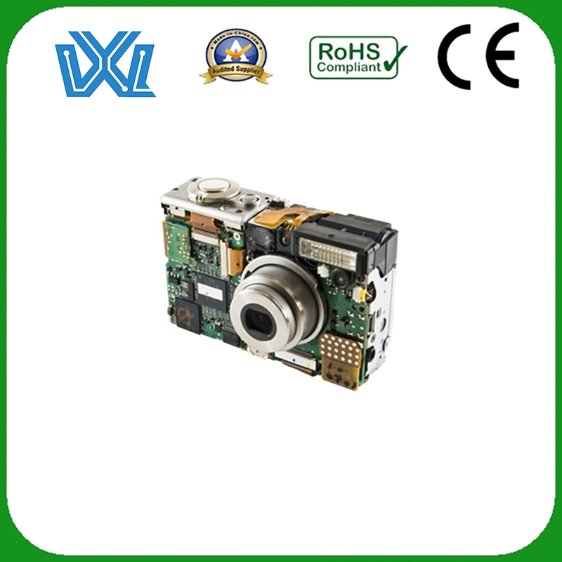
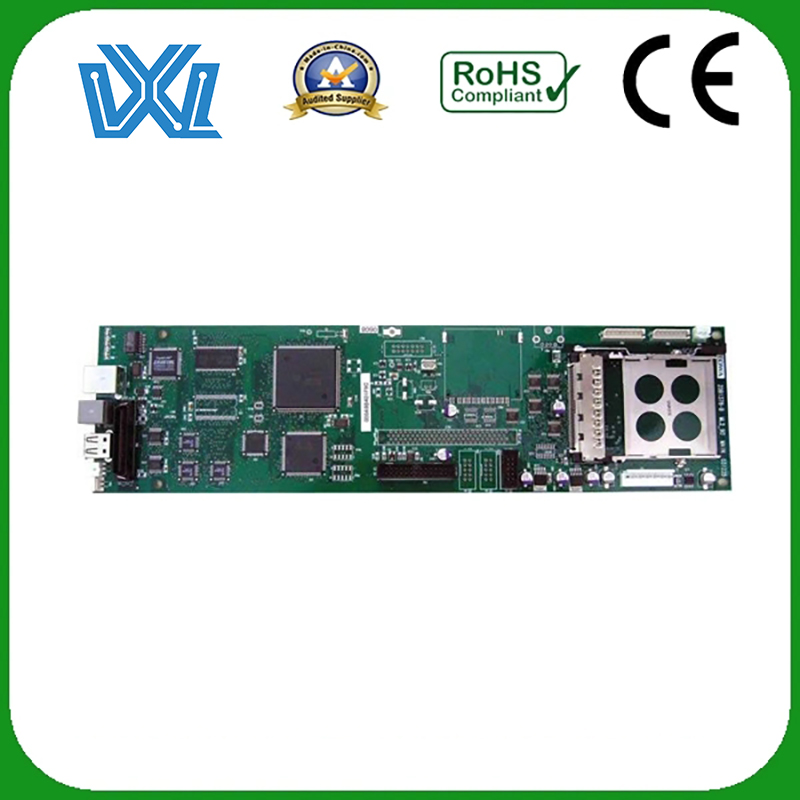
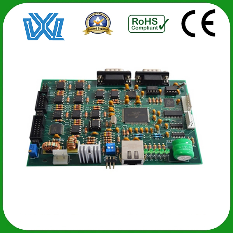
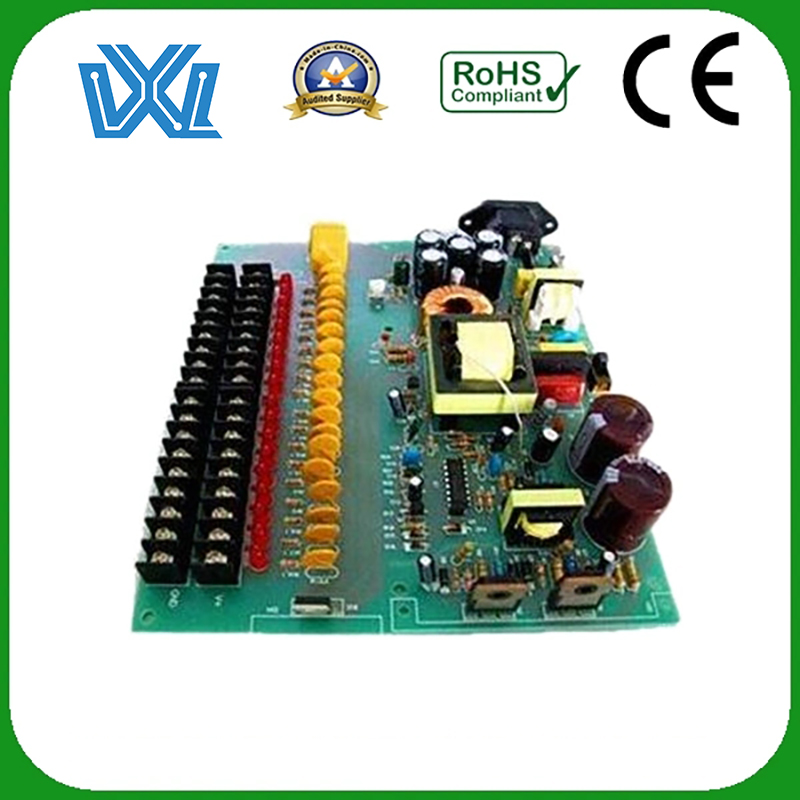
ODM One Sided Pcb Factory - Custom Fr-4 Circuit Board Pcb Board – Weilian Electronics
ODM One Sided Pcb Factory - Custom Fr-4 Circuit Board Pcb Board – Weilian Electronics Detail:
Basic Rules of PCB Layout
1. Layout according to the circuit module, the related circuits that realize the same function are called a module, the components in the circuit module should adopt the principle of nearest concentration, and the digital circuit and the analog circuit should be separated;
2. Components and devices must be mounted within 1.27mm around non-mounting holes such as positioning holes and standard holes, and no components shall be mounted within 3.5mm (for M2.5) and 4mm (for M3) around mounting holes such as screws;
3. Avoid placing vias below components such as horizontally mounted resistors, inductors (plug-ins), and electrolytic capacitors to avoid short circuits between the vias and the component shell after wave soldering;
4. The distance between the outside of the component and the edge of the board is 5mm;
5. The distance between the outside of the mounted component pad and the outside of the adjacent mounted component is greater than 2mm;
6. Metal shell components and metal parts (shielding boxes, etc.) cannot touch other components, and cannot be close to printed lines and pads, and the spacing should be greater than 2mm. The size of the positioning holes, fastener installation holes, elliptical holes and other square holes in the plate is greater than 3mm from the edge of the plate;
7. The heating element cannot be close to the wire and the thermal element; the high-heating element should be evenly distributed;
8. The power socket should be arranged around the printed board as much as possible, and the bus bar terminals connected to the power socket should be arranged on the same side. Special care should be taken not to arrange power sockets and other soldered connectors between the connectors, in order to facilitate the soldering of these sockets and connectors, and the design and tying of power cables. The arrangement spacing of power sockets and welding connectors should be considered to facilitate the insertion and removal of power plugs;
9. Arrangement of other components:
All IC components are unilaterally aligned, the polarity of polar components is clearly marked, and the polarity marking on the same printed board should not be more than two directions. When two directions appear, the two directions are perpendicular to each other;
10. The wiring on the board should be properly dense. When the difference in density is too large, it should be filled with mesh copper foil, and the mesh should be greater than 8mil (or 0.2mm);
11. There should be no through-holes on the patch pads, so as to avoid the loss of solder paste and cause the components to be soldered. Important signal lines are not allowed to pass between the socket pins;
12. The patch is unilaterally aligned, the character direction is the same, and the packaging direction is the same;
13. For devices with polarity, the direction of polarity marking on the same board should be as consistent as possible.
PCB Component Routing Rules
1. In the area where the wiring area is less than or equal to 1mm from the edge of the PCB, and within 1mm around the mounting hole, wiring is prohibited;
2. The power line should be as wide as possible and should not be less than 18mil; the signal line width should not be less than 12mil; the cpu input and output lines should not be less than 10mil (or 8mil); the line spacing should not be less than 10mil;
3. The normal via is not less than 30mil;
4. Dual in-line: pad 60mil, aperture 40mil;
1/4W resistor: 51*55mil (0805 surface mount); when in-line, the pad is 62mil, and the aperture is 42mil;
Electrodeless capacitor: 51*55mil (0805 surface mount); when plugged directly, the pad is 50mil, and the aperture is 28mil;
5.Note that the power wire and the ground wire should be as radial as possible, and the signal wire should not be looped.
Factory Show

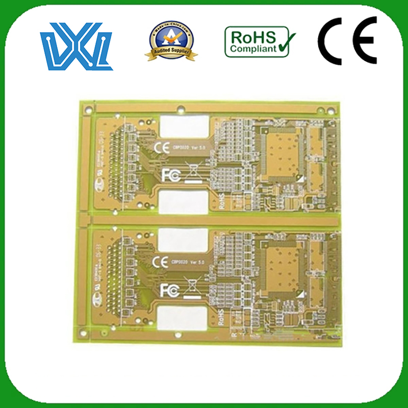
Product detail pictures:


Related Product Guide:
No matter new customer or previous client, We believe in prolonged time period and trustworthy relationship for ODM One Sided Pcb Factory - Custom Fr-4 Circuit Board Pcb Board – Weilian Electronics , The product will supply to all over the world, such as: Iraq, Irish, Nicaragua, As a way to make use of the resource on the expanding information and facts in international trade, we welcome prospects from everywhere on the web and offline. In spite in the top quality products we offer, effective and satisfying consultation service is supplied by our specialist after-sale service group. Solution lists and detailed parameters and any other info weil be sent to you timely for the inquiries. So please get in touch with us by sending us emails or contact us if you have any concerns about our firm. ou can also get our address info from our web site and come to our enterprise. or a field survey of our solutions. We're confident that we are going to share mutual results and build solid co-operation relations with our companions in this market. We're looking forward to your inquiries.
The accounts manager made a detailed introduction about the product, so that we have a comprehensive understanding of the product, and ultimately we decided to cooperate.

