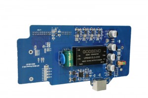
PCBA is the abbreviation of Printed Circuit Board Assembly in English, that is to say, the empty PCB board passes through the SMT upper part, or the whole process of DIP plug-in, referred to as PCBA. This is a commonly used method in China, while the standard method in Europe and America is PCB’ A, add “‘”, which is called the official idiom.
Printed circuit board, also known as printed circuit board, printed circuit board, often uses the English abbreviation PCB (Printed circuit board), is an important electronic component, a support for electronic components, and a provider of circuit connections for electronic components. Because it is made using electronic printing techniques, it is called a “printed” circuit board. Before the appearance of printed circuit boards, the interconnection between electronic components relied on the direct connection of wires to form a complete circuit. Now, the circuit panel only exists as an effective experimental tool, and the printed circuit board has become an absolute dominant position in the electronics industry. At the beginning of the 20th century, in order to simplify the production of electronic machines, reduce the wiring between electronic parts, and reduce the production cost, people began to study the method of replacing wiring with printing. In the past 30 years, engineers have continuously proposed to add metal conductors on insulating substrates for wiring. The most successful was in 1925, Charles Ducas of the United States printed circuit patterns on insulating substrates, and then successfully established conductors for wiring by electroplating.
Until 1936, the Austrian Paul Eisler (Paul Eisler) published the foil film technology in the United Kingdom. He used a printed circuit board in a radio device; Successfully applied for a patent for the method of blowing and wiring (Patent No. 119384). Among the two, Paul Eisler’s method is most similar to today’s printed circuit boards. This method is called the subtraction method, which is to remove unnecessary metal; while the method of Charles Ducas and Miyamoto Kinosuke is to add only the required metal. Wiring is called additive method. Even so, because the electronic components at that time generated a lot of heat, the substrates of the two were difficult to use together, so there was no formal practical use, but it also made the printed circuit technology a step further.
History
In 1941, the United States painted copper paste on talc for wiring to make proximity fuses.
In 1943, Americans used this technology extensively in military radios.
In 1947, epoxy resins began to be used as manufacturing substrates. At the same time, NBS began to study manufacturing technologies such as coils, capacitors, and resistors formed by printed circuit technology.
In 1948, the United States officially recognized the invention for commercial use.
Since the 1950s, transistors with lower heat generation have largely replaced vacuum tubes, and printed circuit board technology has only begun to be widely used. At that time, etching foil technology was the mainstream.
In 1950, Japan used silver paint for wiring on glass substrates; and copper foil for wiring on paper phenolic substrates (CCL) made of phenolic resin.
In 1951, the appearance of polyimide made the heat resistance of the resin a step further, and polyimide substrates were also manufactured.
In 1953, Motorola developed a double-sided plated through-hole method. This method is also applied to later multi-layer circuit boards.
In the 1960s, after the printed circuit board was widely used for 10 years, its technology became more and more mature. Since Motorola’s double-sided board came out, multilayer printed circuit boards began to appear, which increased the ratio of wiring to substrate area.
In 1960, V. Dahlgreen made a flexible printed circuit board by pasting a metal foil film printed with a circuit in a thermoplastic plastic.
In 1961, the Hazeltine Corporation of the United States referred to the electroplating through-hole method to produce multi-layer boards.
In 1967, “Plated-up technology”, one of the layer-building methods, was published.
In 1969, FD-R manufactured flexible printed circuit boards with polyimide.
In 1979, Pactel published the “Pactel method”, one of the layer-adding methods.
In 1984, NTT developed the “Copper Polyimide Method” for thin-film circuits.
In 1988, Siemens developed the Microwiring Substrate build-up printed circuit board.
In 1990, IBM developed the “Surface Laminar Circuit” (Surface Laminar Circuit, SLC) build-up printed circuit board.
In 1995, Matsushita Electric developed ALIVH’s build-up printed circuit board.
In 1996, Toshiba developed B2it’s build-up printed circuit board.
Post time: Feb-24-2023

