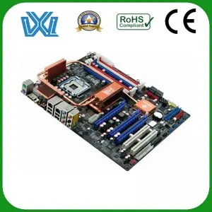
Printed circuit boards (PCBs) are the backbone of modern electronic devices. From smartphones to medical devices, PCB boards play a vital role in connecting and providing functionality to various electronic components. To ensure optimal performance, PCB designers must consider several factors, including controlled impedance. In this blog post, we will delve into the concept of controlled impedance in PCB boards and understand its importance for achieving efficient and reliable circuit designs.
What is controlled impedance in PCB?
Impedance can be defined as the resistance encountered by alternating current (AC) flowing through a circuit. Controlled impedance specifically refers to an intentionally consistent impedance value on a specific trace or transmission line on a PCB board.
Impedance control is critical when processing high-frequency digital signals because it helps maintain signal integrity, minimize signal reflections, and reduce electromagnetic interference (EMI). When impedance is not controlled, it can destroy the transmission characteristics of the signal, causing distortion, timing issues, and overall performance degradation.
Factors affecting controlled impedance:
In order to achieve controlled impedance of the PCB board, several factors need to be considered. These factors include:
1. Trace geometry: The width, thickness and spacing of traces and transmission lines on the PCB have a great influence on the impedance value. Dimensions must be accurately calculated using an impedance calculator or provided by the PCB manufacturer.
2. Dielectric material: The dielectric material used in the PCB also affects the controlled impedance. Different materials have different dielectric constants, which affects how quickly signals propagate.
3. Distance of adjacent traces: The proximity of transmitting and receiving traces will cause mutual capacitance and mutual inductance, thereby changing the impedance value. Maintaining a safe distance between traces helps maintain controlled impedance.
4. Layer stacking: The arrangement and sequence of PCB layers play a vital role in impedance control. Consistency in layer stacking is critical to preventing impedance inconsistencies.
The importance of controlled impedance in PCB design:
1. Signal integrity: Controlled impedance ensures that digital signals are transmitted effectively in the PCB without distortion. Maintaining impedance control minimizes reflections, signal loss, and crosstalk, thereby improving overall signal integrity.
2. Reduce electromagnetic interference (EMI): As electronic devices continue to increase in complexity and signal frequencies become higher, EMI has become an important issue. Controlled impedance helps minimize EMI by reducing signal reflections and ensuring proper grounding and shielding.
3. Consistent performance: PCBs with controlled impedance provide consistent electrical characteristics even under changing environmental conditions such as temperature and humidity. This consistency translates into reliable performance and extended life of your electronic devices.
4. Compatibility: Controlled impedance also ensures compatibility with other components and systems. PCB boards with impedance matching can easily connect and communicate with other devices, allowing for seamless integration.
Controlled impedance is a critical aspect of PCB design, especially for high frequency and sensitive applications. By maintaining consistent impedance values, designers can optimize signal integrity, reduce EMI, and ensure compatibility. Understanding the factors that affect controlled impedance, such as trace geometry, dielectric materials, and layer stackup, is critical to achieving efficient and reliable PCB designs. By prioritizing impedance control, designers can unlock the full potential of electronic devices while delivering superior performance and longevity.
Post time: Sep-15-2023

