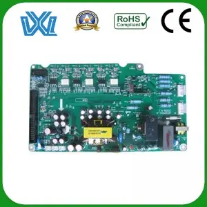
The PCB board manufacturing process can be roughly divided into the following twelve steps. Each process requires a variety of process manufacturing. It should be noted that the process flow of boards with different structures is different. The following process is the complete production of multi-layer PCB. process flow;
First. Inner layer; mainly for making the inner layer circuit of PCB circuit board; the production process is:
1. Cutting board: cutting the PCB substrate into production size;
2. Pre-treatment: clean the surface of the PCB substrate and remove surface pollutants
3. Laminating film: paste the dry film on the surface of the PCB substrate to prepare for the subsequent image transfer;
4. Exposure: Use exposure equipment to expose the film-attached substrate with ultraviolet light, so as to transfer the image of the substrate to the dry film;
5. DE: The substrate after exposure is developed, etched, and film removed, and then the production of the inner layer board is completed.
Second. Internal inspection; mainly for testing and repairing board circuits;
1. AOI: AOI optical scanning, which can compare the image of the PCB board with the data of the good product board that has been entered, so as to find the gaps, depressions and other bad phenomena on the board image;
2. VRS: The bad image data detected by AOI will be sent to VRS for overhaul by relevant personnel.
3. Supplementary wire: Solder the gold wire on the gap or depression to prevent electrical failure;
Third. Pressing; as the name implies, multiple inner boards are pressed into one board;
1. Browning: Browning can increase the adhesion between the board and the resin, and increase the wettability of the copper surface;
2. Riveting: Cut the PP into small sheets and normal size to make the inner board and the corresponding PP fit together
3. Overlapping and pressing, shooting, gong edging, edging;
Fourth. Drilling: according to customer requirements, use a drilling machine to drill holes with different diameters and sizes on the board, so that the holes between the boards can be used for subsequent processing of plug-ins, and it can also help the board to dissipate heat;
Fifth, primary copper; copper plating for the drilled holes of the outer layer board, so that the lines of each layer of the board are conducted;
1. Deburring line: remove the burrs on the edge of the board hole to prevent poor copper plating;
2. Glue removal line: remove the glue residue in the hole; in order to increase the adhesion during micro-etching;
3. One copper (pth): Copper plating in the hole makes the circuit of each layer of the board conduction, and at the same time increases the copper thickness;
Sixth, the outer layer; the outer layer is roughly the same as the inner layer process of the first step, and its purpose is to facilitate the follow-up process to make the circuit;
1. Pre-treatment: Clean the surface of the board by pickling, brushing and drying to increase the adhesion of the dry film;
2. Laminating film: paste the dry film on the surface of the PCB substrate to prepare for the subsequent image transfer;
3. Exposure: irradiate with UV light to make the dry film on the board form a polymerized and unpolymerized state;
4. Development: dissolve the dry film that has not been polymerized during the exposure process, leaving a gap;
Seventh, secondary copper and etching; secondary copper plating, etching;
1. Second copper: Electroplating pattern, cross chemical copper for the place not covered with dry film in the hole; at the same time, further increase the conductivity and copper thickness, and then go through tin plating to protect the integrity of the circuit and holes during etching;
2. SES: Etch the bottom copper in the attachment area of the outer layer dry film (wet film) through processes such as film removal, etching, and tin stripping, and the outer layer circuit is now completed;
Eighth, solder resistance: it can protect the board and prevent oxidation and other phenomena;
1. Pretreatment: pickling, ultrasonic washing and other processes to remove oxides on the board and increase the roughness of the copper surface;
2. Printing: Cover the parts of the PCB board that do not need to be soldered with solder resist ink to play the role of protection and insulation;
3. Pre-baking: drying the solvent in the solder resist ink, and at the same time hardening the ink for exposure;
4. Exposure: Curing the solder resist ink by UV light irradiation, and forming a high molecular polymer through photopolymerization;
5. Development: remove the sodium carbonate solution in the unpolymerized ink;
6. Post-baking: to fully harden the ink;
Ninth, text; printed text;
1. Pickling: Clean the surface of the board, remove surface oxidation to strengthen the adhesion of printing ink;
2. Text: printed text, convenient for subsequent welding process;
Tenth, surface treatment OSP; the side of the bare copper plate to be welded is coated to form an organic film to prevent rust and oxidation;
Eleventh, forming; the shape of the board required by the customer is produced, which is convenient for the customer to carry out SMT placement and assembly;
Twelfth, flying probe test; test the circuit of the board to avoid the outflow of the short circuit board;
Thirteenth, FQC; final inspection, sampling and full inspection after completing all processes;
Fourteenth, packaging and out of the warehouse; vacuum-pack the finished PCB board, pack and ship, and complete the delivery;
Post time: Apr-24-2023

