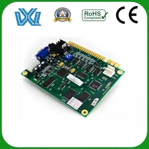
The process of converting a circuit diagram into a functional printed circuit board (PCB) layout can be a daunting task, especially for beginners in electronics. However, with the right knowledge and tools, creating a PCB layout from a schematic can be an enjoyable and rewarding experience. In this blog, we will explore the steps involved in making a PCB layout from a circuit diagram, providing you with valuable insights to master the art of PCB layout design.
Step 1: Know the Circuit Diagram
A thorough understanding of the circuit diagram is crucial before diving into PCB layout design. Identify the components, their connections, and any specific requirements for the design. This will enable you to plan and execute layouts efficiently.
Step 2: Transmission Circuit Diagram
To start the layout design process, you need to transfer the schematic to your PCB design software. There are a variety of software options on the market, both free and paid, with varying degrees of sophistication. Choose the one that suits your requirements and expertise.
Step 3: Component Placement
The next step is to place the components on the PCB layout. Several factors are considered when laying out components, such as signal paths, power connections, and physical constraints. Organize your layout in a way that ensures minimal disruption and optimal performance.
Step Four: Wiring
After placing components, the next critical step is routing. Traces are copper pathways that connect components on a PCB. Route critical signals first, such as high frequency or sensitive lines. Use proper design techniques, such as avoiding sharp angles and crossing traces, to minimize crosstalk and interference.
Step 5: Ground and Power Planes
Integrate proper ground and power planes into the PCB layout design. The ground plane provides a low-resistance return path for current, reducing noise and improving signal integrity. Likewise, power planes help distribute power evenly across the board, minimizing voltage drop and increasing efficiency.
Step 6: Design Rule Check (DRC)
After layout is complete, a Design Rule Check (DRC) must be performed. DRC checks your design against predefined rules and specifications, ensuring that the layout meets the required standards. Be aware of clearances, trace widths, and other design parameters during this process.
Step 7: Generate Manufacturing Files
After successfully passing the DRC, manufacturing files can be generated. These files include Gerber files and a Bill of Materials (BOM), which contains the data required for PCB fabrication, listing all the components required for the assembly process. Ensure manufacturing documentation is accurate and meets manufacturer’s requirements.
in conclusion:
Designing a PCB layout from a schematic involves a systematic approach from understanding the circuit to generating manufacturing documentation. Every step in the process requires attention to detail and careful planning. By following these steps and taking advantage of the tools and software available, you can master the art of PCB layout design and bring your schematics to life. So roll up your sleeves and let your creativity and technical skills run wild in the world of PCB design!
Post time: Jul-17-2023

