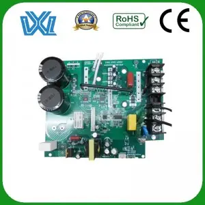
Welcome to our comprehensive guide on how to make a PCB (Printed Circuit Board)! In this blog post, we’ll walk you through the process of creating a PCB from scratch, providing step-by-step instructions and helpful tips along the way. Whether you are a hobbyist, student, or aspiring electronics enthusiast, this guide is tailored to help you successfully design and manufacture your own PCBs. So, let’s take a deeper look!
1. Understand the basics of PCB design:
Before we get into the manufacturing process, it is crucial to have a solid understanding of the basics of PCB design. Become familiar with the necessary software tools, such as EDA (Electronic Design Automation) software, which enables you to create and layout circuit designs.
2. Scheme design:
Begin by conceptualizing your circuit using a schematic. This critical step enables you to plan where each component will be placed on the board. Throughout this phase, ensure that the schematic follows best practices for a clear and concise representation.
3. Create the PCB design:
Once the schematic is ready, it is transferred to the PCB design software. Components are placed on the board first, taking care to organize them optimally for efficient routing. Remember to consider factors such as component size, connectivity, and thermal dissipation.
4. Routing:
Routing involves creating traces or conductive paths to connect various components on a PCB. Carefully determine the routing of each trace, considering factors such as signal integrity, power distribution, and ground planes. Pay close attention to clearance rules and make sure your designs meet standard manufacturing tolerances.
5. Design verification:
Your design must be thoroughly validated before proceeding with the manufacturing process. Do a Design Rule Check (DRC) and check your layout from every angle. Make sure the traces are properly separated and there are no potential shorts.
6. Production process:
Once you are satisfied with your PCB design, the manufacturing process can begin. Start by transferring your design to the copper clad board using a pre-coated PCB or toner transfer method. Etch the board to remove excess copper, leaving only the required traces and pads.
7. Drilling and plating:
Using a small drill bit, carefully drill holes in the designated locations on the PCB. These holes are used to mount components and make electrical connections. After drilling, the holes are plated with a thin layer of conductive material such as copper to enhance conductivity.
8. Welding components:
Now it’s time to assemble the components onto the PCB. Solder each component in place, ensuring proper alignment and good solder joints. It is recommended to use a soldering iron with proper power and temperature to protect the components and PCB.
9. Testing and Troubleshooting:
After soldering is complete, it is critical to test the functionality of the PCB. Use a multimeter or appropriate test equipment to check for connectivity, voltage levels and potential faults. Fix any problems that arise and make necessary adjustments or replace components.
in conclusion:
Congratulations! You just learned how to make a PCB from scratch. By following this comprehensive guide, you can now design, manufacture and assemble your own printed circuit boards. PCB fabrication is a fascinating yet challenging process that requires attention to detail, patience and knowledge of electronics. Remember to experiment and accept the learning curve. With practice, you will gain confidence and be able to create increasingly complex PCB designs. Happy PCB making!
Post time: Jun-24-2023

