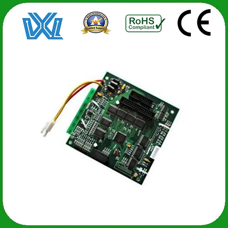
The PCB circuit board is constantly changing with the progress of the process technology, but in principle, a complete PCB circuit board needs to print the circuit board, then cut the circuit board, process the copper clad laminate, transfer the circuit board, Corrosion, drilling, pretreatment, and welding can only be powered on after these production processes. The following is a detailed understanding of the PCB circuit board production process.
Design the schematic diagram according to the circuit function needs. The design of the schematic diagram is mainly based on the electrical performance of each component to be reasonably constructed as needed. The diagram can accurately reflect the important functions of the PCB circuit board and the relationship between the various components. The design of the schematic diagram is the first step in the PCB production process, and it is also a very important step. Usually the software used to design circuit schematics is PROTEl.
After the schematic design is completed, it is necessary to further package each component through PROTEL to generate and realize a grid with the same appearance and size of components. After modifying the component package, execute Edit/Set Preference/pin 1 to set the package reference point at the first pin. Then execute Report/Component Rule check to set all the rules to be checked, and OK. At this point, the package is established.
Formally generate the PCB. After the network is generated, the position of each component needs to be placed according to the size of the PCB panel, and it is necessary to ensure that the leads of each component do not cross when placing. After the placement of components is completed, DRC inspection is finally carried out to eliminate pin or lead crossing errors of each component during wiring. When all errors are eliminated, a complete pcb design process is completed.
Print circuit board: Print out the drawn circuit board with transfer paper, pay attention to the slippery side facing yourself, generally print two circuit boards, that is, print two circuit boards on one paper. Among them, choose the one with the best printing effect to make the circuit board.
Cut the copper clad laminate, and use the photosensitive plate to make the whole process diagram of the circuit board. Copper-clad laminates, that is, circuit boards covered with copper film on both sides, cut the copper-clad laminates into the size of the circuit board, not too large, to save materials.
Pretreatment of copper clad laminates: use fine sandpaper to polish off the oxide layer on the surface of copper clad laminates to ensure that the toner on the thermal transfer paper can be firmly printed on the copper clad laminates when transferring the circuit board. Shiny finish with no visible stains.
Transfer printed circuit board: Cut the printed circuit board into a suitable size, paste the printed circuit board side on the copper clad laminate, after alignment, put the copper clad laminate into the thermal transfer machine, and ensure the transfer when putting it in Paper is not misaligned. Generally speaking, after 2-3 transfers, the circuit board can be firmly transferred to the copper clad laminate. The thermal transfer machine has been preheated in advance, and the temperature is set at 160-200 degrees Celsius. Due to the high temperature, please pay attention to safety when operating!
Corrosion circuit board, reflow soldering machine: first check whether the transfer is complete on the circuit board, if there are a few places that are not transferred well, you can use a black oil-based pen to repair. Then it can be corroded. When the copper film exposed on the circuit board is completely corroded, the circuit board is taken out from the corrosive liquid and cleaned, so that a circuit board is corroded. The composition of the corrosive solution is concentrated hydrochloric acid, concentrated hydrogen peroxide, and water in a ratio of 1:2:3. When preparing the corrosive solution, add water first, then add concentrated hydrochloric acid and concentrated hydrogen peroxide. If the concentrated hydrochloric acid, concentrated hydrogen peroxide or corrosive solution does not Be careful to splash on the skin or clothing and wash it with clean water in time. Since a strong corrosive solution is used, be sure to pay attention to safety when operating!
Circuit board drilling: The circuit board is to insert electronic components, so it is necessary to drill the circuit board. Choose different drills according to the thickness of the pins of electronic components. When using a drill to drill holes, the circuit board must be pressed firmly. The speed of the drill should not be too slow. Please watch the operator carefully.
Circuit board pretreatment: After drilling, use fine sandpaper to polish off the toner covering the circuit board, and clean the circuit board with clean water. After the water is dry, apply pine water to the side with the circuit. In order to speed up the solidification of the rosin, we use a hot air blower to heat the circuit board, and the rosin can solidify in only 2-3 minutes.
Welding electronic components: After the welding work is completed, conduct a comprehensive test on the entire circuit board. If there is a problem during the test, it is necessary to determine the location of the problem through the schematic diagram designed in the first step, and then re-solder or replace the component. device. When the test is passed successfully, the whole circuit board is finished.
Post time: May-15-2023

